- 您现在的位置:买卖IC网 > Sheet目录503 > RFRXD0920-I/LQ (Microchip Technology)MODULE RCVR 868/915MHZ ASK/FSK
�� �
�
�rfRXD0420/0920�
�3.2.2.1�
�DYNAMIC� REFERENCE� VOLTAGE�
�Selection� of� component� values� for� R1� and� C2� is� an�
�A� dynamic� reference� voltage� can� be� derived� by� averag-�
�ing� the� received� signal� with� a� low-pass� filter.� The� exam-�
�ple� ASK� application� circuit� shown� in� Figure� 3-9,� the�
�low-pass� filter� is� formed� by� R1� and� C2.� The� output� of�
�the� low-pass� filter� is� then� fed� to� OPA-.�
�The� setting� of� the� R1-C2� time� constant� depends� on� the�
�ratio� of� logical� ones� versus� zeros� and� a� trade� off� in�
�stability� versus� receiver� reaction� time.� If� the� received�
�signal� has� an� even� number� of� logical� ones� versus�
�zeros,� the� time� constant� can� be� set� relatively� short.�
�Thus� the� reference� voltage� can� react� quickly� to�
�changes� in� the� received� signal� amplitude� and� differ-�
�ences� in� transmitters.� However,� it� may� not� be� as� stable�
�and� can� fluctuate� with� the� ratio� of� logical� ones� and�
�iterative� process.� First� start� with� a� time� constant�
�between� 10� to� 100� times� the� signal� rate.� Second,� view�
�the� reference� voltage� against� the� RSSI� signal� to�
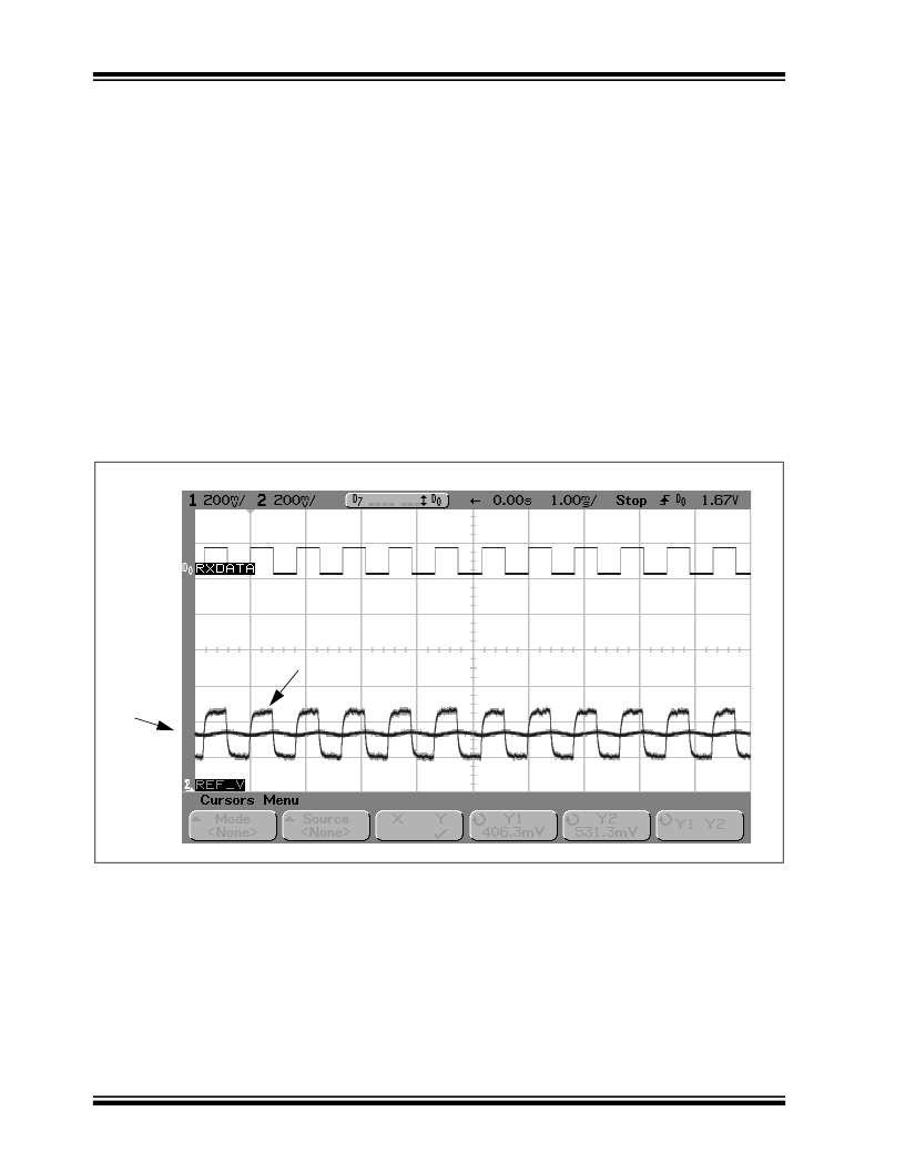
�determine� if� the� values� are� suitable.� Figure� 3-12� is� an�
�oscilloscope� screen� capture� of� an� incoming� RF� square�
�wave� modulated� signal� (ASK� on-off� keying).� The� top�
�trace� is� the� data� output� of� OPA� (Pin� 18).� The� two�
�bottom� traces� are� the� RSSI� signal� (Pin� 21,� bottom�
�square� wave)� and� generated� reference� voltage� (Pin� 19,�
�bottom� trace� centered� in� the� RSSI� square� wave).� The�
�goal� is� to� select� values� for� R1� and� C2� such� that� the�
�reference� voltage� is� in� the� middle� of� the� RSSI� signal.�
�This� reference� voltage� level� provides� the� optimum� data�
�comparison� of� the� incoming� data� signal.�
�zeros.� If� the� time� constant� is� set� long,� the� reference�
�3.2.2.2�
�STATIC� REFERENCE� VOLTAGE�
�voltage� will� be� more� stable.� However,� the� receiver�
�cannot� react� as� quickly� upon� the� reception� of� a�
�received� signal.�
�A� static� reference� voltage� can� be� derived� by� a� voltage�
�divider� network.�
�FIGURE� 3-12:�
�RSSI� AND� REFERENCE� VOLTAGE� COMPARISON�
�OPA�
�(Pin� 18)�
�RSSI�
�OPA-�
�(Pin� 19)�
�(Pin� 21)�
�DS70090A-page� 16�
�Preliminary�
�?� 2003� Microchip� Technology� Inc.�
�发布紧急采购,3分钟左右您将得到回复。
相关PDF资料
RHK005N03T146
MOSFET N-CH 30V 500MA SOT-346
RHP020N06T100
MOSFET N-CH 60V 2A SOT-89
RHP030N03T100
MOSFET N-CH 30V 3A SOT-89
RI-TRP-WEHP-30
RFID GLASS TRANSP R/W 80BIT 23MM
RJ45-XLRM
CONVERTER LEAD RJ45-XLR MALE
RJK005N03T146
MOSFET N-CH 30V 500MA SOT-346
RJK0230DPA-00#J5A
MOSFET DL N-CH 25V 20A WPAK
RJK0353DSP-00#J0
MOSFET N-CH 30V 18A 8-SOP
相关代理商/技术参数
RFRXD0920T-I/LQ
功能描述:射频收发器 32 LD 800-930 MHz RF RoHS:否 制造商:Atmel 频率范围:2322 MHz to 2527 MHz 最大数据速率:2000 Kbps 调制格式:OQPSK 输出功率:4 dBm 类型: 工作电源电压:1.8 V to 3.6 V 最大工作温度:+ 85 C 接口类型:SPI 封装 / 箱体:QFN-32 封装:Tray
RFS04ZG-M6
制造商:Power-One 功能描述:
RFS04ZG-M6G
制造商:Power-One 功能描述:RFS Series 20 W Single Output 5 V DC/DC Converter Power Supply - Surface Mount
RFS062PJ150CS
功能描述:RES ARRAY 2 RES 15 OHM 0603 制造商:samsung electro-mechanics 系列:RFS 包装:剪切带(CT) 零件状态:在售 电路类型:隔离 电阻(欧姆):15 容差:±5% 电阻器数:2 引脚数:4 每元件功率:31.25mW 温度系数:±200ppm/°C 工作温度:-55°C ~ 125°C 应用:- 安装类型:表面贴装 封装/外壳:0302(0805 公制),长边端子 供应商器件封装:603 大小/尺寸:0.032" 长 x 0.024" 宽(0.80mm x 0.60mm) 高度 - 安装(最大值):0.013"(0.33mm) 标准包装:1
RFS062PJ220CS
功能描述:RES ARRAY 2 RES 22 OHM 0603 制造商:samsung electro-mechanics 系列:RFS 包装:剪切带(CT) 零件状态:在售 电路类型:隔离 电阻(欧姆):22 容差:±5% 电阻器数:2 引脚数:4 每元件功率:31.25mW 温度系数:±200ppm/°C 工作温度:-55°C ~ 125°C 应用:- 安装类型:表面贴装 封装/外壳:0302(0805 公制),长边端子 供应商器件封装:603 大小/尺寸:0.032" 长 x 0.024" 宽(0.80mm x 0.60mm) 高度 - 安装(最大值):0.013"(0.33mm) 标准包装:1
RFS062PJ240CS
功能描述:RES ARRAY 2 RES 24 OHM 0603 制造商:samsung electro-mechanics 系列:RFS 包装:剪切带(CT) 零件状态:在售 电路类型:隔离 电阻(欧姆):24 容差:±5% 电阻器数:2 引脚数:4 每元件功率:31.25mW 温度系数:±200ppm/°C 工作温度:-55°C ~ 125°C 应用:- 安装类型:表面贴装 封装/外壳:0302(0805 公制),长边端子 供应商器件封装:603 大小/尺寸:0.032" 长 x 0.024" 宽(0.80mm x 0.60mm) 高度 - 安装(最大值):0.013"(0.33mm) 标准包装:1
RFS062PJ270CS
功能描述:RES ARRAY 2 RES 27 OHM 0603 制造商:samsung electro-mechanics 系列:RFS 包装:剪切带(CT) 零件状态:在售 电路类型:隔离 电阻(欧姆):27 容差:±5% 电阻器数:2 引脚数:4 每元件功率:31.25mW 温度系数:±200ppm/°C 工作温度:-55°C ~ 125°C 应用:- 安装类型:表面贴装 封装/外壳:0302(0805 公制),长边端子 供应商器件封装:603 大小/尺寸:0.032" 长 x 0.024" 宽(0.80mm x 0.60mm) 高度 - 安装(最大值):0.013"(0.33mm) 标准包装:1
RFS062PJ300CS
制造商:Samsung Electro-Mechanics 功能描述:- Tape and Reel